[ad_1]

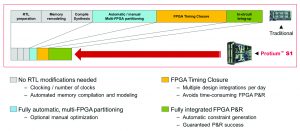
Figure 1: Cadence’s Protium S1 FPGA-based prototyping platform cuts the time it takes to verify SoC code
With ever-increasing embedded software content in complex system‑on‑chip (SoC) devices, it has become crucial to develop and to verify software and hardware concurrently, and as early as possible in the design cycle.
FPGA-based prototyping plays an increasingly important role in this, because it satisfies the speed requirements of concurrent verification better than any other tool available.
It has historically taken a long time to get the prototype up and running, so users are still cautious when it comes to deploying FPGA-based prototyping.
Nevertheless, once the prototype is operational it can be a pre-production version of the actual chip and system, giving the user a true hardware and software verification and integration platform.
What’s holding things up?
So why has prototyping been hard to do until now?
Major issues that have faced designers working on FPGA-based prototyping are:
- Complex ASIC clocking, with hundreds or even thousands of clocks, gated clocks and multiplexed clocks, exceeding the capabilities of FPGAs.
- Difficulty mapping ASIC memories with different numbers of ports, array sizes, data bus and address bus widths into the fixed structure of two-port FPGA memories.
- Appropriate hardware and software debug requirements that have to be met when the FPGA-based prototype is used as a verification tool.
These issues lead to prototyping bring-up times that are usually measured in months, which is a long time in today’s fast-paced industry.
Typically, FPGA prototyping platforms require significant changes to the ASIC register-transfer level (RTL). This is a disadvantage for two reasons: it is time consuming; and the design is close to, but not exactly the same as, the one in ASIC.
Therefore, a prototyping solution is needed that requires virtually no changes to the ASIC RTL, to ensure that the design that is running on the FPGA is exactly the design that was intended.
Clock implementation
To be able to guarantee FPGA timing closure by construction, a proprietary clock implementation technology that removes all FPGA hold-time violations, and eliminates all FPGA clocking limitations, is crucial for a smooth design implementation.
This clocking technology serves as a foundation to provide many advanced use modes and debug capabilities. Cadence’s Protium S1 FPGA-based prototyping platform offers one approach to solving these challenges.
Another innovative technology in the platform is the integrated memory compiler, that automatically maps ASIC memories of different ports, sizes and widths, on to the two-port memories available in FPGAs.
The memory compiler also works with external bulk memories on physical memory daughter-cards to expand the amount of memory that is available in the FPGA in two ways:
- It has an external SRAM card that is 100% transparent to the user, and increases the FPGA memory from 80Mbits to 128Mbytes.
- It has an external DRAM card containing 16GBytes of DDR memory, featuring a separate FPGA that acts as a memory SpeedBridge, and a memory protocol converter, making the 16GB DDR memory look to the user design like a LPDDR2/3/4, DDR3/4, HBM, or UFS, for instance.
Debug requirements
Debug on an FPGA-based prototype falls into two major categories. First, hardware debug is mostly used to bring up the prototype, and to debug unexpected behaviour during runtime.
This requirement can be addressed in the prototyping platform by:
- Waveform capture and view across FPGAs.
- Capability to force internal signals into “0” or “1” and release when desired.
- Real-time monitoring of key signals.
Software debug is the other main use mode for FPGA-based prototyping. Supporting it requires a different set of capabilities:
- JTAG and UART ports.
- Backdoor memory access to read and write the content of any memory, for example to upload a new boot code.
- Full clock control to stop and resume clock as desired.
- Full remote access to the Protium S1 system.
ASIC designers have found FPGA‑based prototyping a challenge to implement, due to various issues that take months to resolve.
Having a solution at hand that cuts the bring-up time from several months to a couple of weeks by automating most of the process, will accelerate time-to-market by months.
[ad_2]
Source link

