[ad_1]
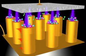
The technique involves constructing a ~1nm gap between two metal electrodes (see diagram), and then using a potential difference to promote electron tunnelling across the gap.
This tunnelling occurs in two forms: elastic and inelastic, King’s physicist Dr Pan Wang told Electronics Weekly.
In-elastic tunnelling (across top gap in diagram) is lossy, loosing energy in the form of plasmons which the process excites in the receiving electrode (gold nano-rod in the diagram).
These plasmons, said Wang, are collective oscillations of electrons in the surface of the metallic rods, oscillating at optical frequencies.
When they reach the far (lower) end of the rod, they couple into free-space as photons – light – at the optical frequency.
The wavelength of which is directly related to the applied voltage.
“For optical interconnect,” said Wang, “this is an alternative to semiconductor lasers. Semiconductor lasers are big, and also not CMOS-compatible.”
Due to the small size of the parts concerned, rapid modulation of the output light is believed to be possible.
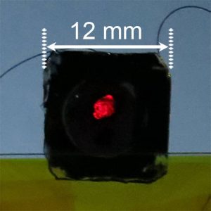
Light emission is very inefficient as most tunnelling across the gap is elastic (see below), but the King’s meta-material gold rod array provides a hundred billion tunnel junctions that convert so many electrons to plasmons that the light emitted is visible to the naked eye (see photo).
Elastic tunnelling
Unlike in-elastic tunnelling, elastic tunnelling is efficient and does not form plasmons. Instead it creates ‘hot’ (high-energy) electrons in the gap.
If there are molecules in the gap, chemical reactions can be promoted by these hot electrons, opening the door to scientific and sensing applications.
At the same time, if the amount of in-elastic tunnelling is affected by the reaction or the molecules, the amount of light emitted at the far end of the rods can be used as a measure of the chemistry, said Wang.
To demonstrate the device, the team performed oxidisation and reduction reactions on oxygen and hydrogen molecules.
“The new tunnelling technique allows tunable consistent production of hot electrons and so can be used to control chemical reactions with great precision. Products from a chemical reaction in the junctions will dramatically affect the tunnelling properties,” said Kings College, “The material can be modified to be sensitive to different molecules, making it viable as a sensitive, cheap, and easy to use sensor which provides visual feedback when a molecule is detected.”
The vertical brush-like structure used by the King’s team would allow multiple gaps to be addressed electronically, or horizontal structures could be formed with two electrodes and one gap, said Wang.
The work is published in Nature Nanotechnology as ‘Reactive tunnel junctions in electrically driven plasmonic nanorod metamaterials’.
Happy accident
Chemical research applications were not originally envisaged.
“When we began these studies we expected to generate some weak light which we thought should be enough for various nano-photonic applications on a chip,” said Professor Anatoly Zayats. “But we believe the potential of the approach for designing chemical reactions stimulated with hot electrons and monitoring chemical processes for drug and materials discovery is huge.”
[ad_2]
Source link


