[ad_1]
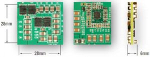
Power density up to 4,000W/in3 is claimed.
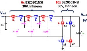
The main application foreseen for the chip, the LTC7820, is 48V non-isolated dc bus conversion, although it is capable of up, down and inverting conversion at a variety of ratios. An example (see diagram below) is a 50A 54 to 9V (6:1) converter peaking at 98% efficiency at 20A.
“Two LTC7820 IC’s can be cascaded for a 4:1 step-down ratio,” said ADI. “For even higher step-down ratios, such as a 6:1, the Dickson converter topology is recommended and is ideal for 54V input to a 9V outputs, requiring only a single LTC7820. ”
 6:1 down conversion at up to 98% efficiency
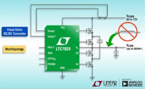
At least four external n-channel mosfets are required, for which the chip includes four powerful (1.1Ω) gate drivers.
Vin max for divide-by-two is 72V, while for doubling and inversion it is 36V. Minimum operating voltage is 6V.
An separate power pin allows the chip to be powered from the stepped-down output, or other available sources up to 40V, reducing power dissipation and improving efficiency.
Switching frequency range is 100kHz to 1MHz.
 Other features include: soft-start, input current sensing and protection for: over-current, short-circuit, over-voltage and under-voltage.
“It stops switching and pulls the /Fault pin low when a fault condition occurs,” said ADI. “An on-board timer can be set for appropriate re-start/re-try times.”
Package is 4 x 5mm QFN-28, and it operates across -40 to 125°C.
Update:
Electronics Weekly contacted the LTC7820 team at Analog Devices to find out more about this novel device.
For example with low-impedance switches connecting capacitors, how are huge current impulses avoided?
It transpires that, before switching starts, the chip pre-charges the power transfer capacitors.
For example, in a divide-by-two application, the flying capacitor bank is alternately switched in series and in parallel with the output capacitor bank, so the circuit pre-charges them both to half the input voltage, with the two capacitor banks equal within, say, 500mV or 1V. The actual window is programmable.
According to the engineers, they did a lot of bench work to ensure the scheme works whatever the input voltage and whatever the initial imbalance.
For it to work, the load on the output has to be small (<50mA), which can be achieved either by shutting down the downstream dc-dc converter, or with an external output disconnect mosfet. A pin on the chip is available to control either of these options.
Another option is to start switching with no voltage on the input, and then ramp up the input voltage, using a hot-swap controller, for example. This approach has to be used for the 6:1 converter above as pre-charge is not available. An LTC4260 hot-swap controller will work from 8 to 80V, it was pointed out.
In this situation, the LTC7820 still does over-voltage and under-voltage detection, and for shut-down the hot-swap controller can be used.
A note on the 6:1 converter, is that it is more efficient – at ~97% – than cascading stages to get the same result.
Why was the chip designed in the first place?
Simply for size, and efficiency, said the team. It comes out 50% smaller than a magnetic-based isolated dc-dc brick converter (although isolation is not available with the switched capacitor option) and dissipates less heat.
What about RFI?
Apparently, all four switches are soft-switched, and the voltage-equalising pre-charge means “there is a current impulse, but the voltage difference is so small you don’t see much of an impulse,” Electronics Weekly was told. And “it is not like a buck converter, there no high-voltage ringing”.
Are the capacitors special?
No, they are low-ESR 1210 (2.5 x 3.5mm) ceramic caps: six off 10µF 50V.
 And is there anything that the team was pleased with?
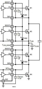
Yes, the top three mosfets get their high-side drives fed through a simple three-diode arrangement (right). “We use simplest elegant way – three diodes. Nobody else has done that, so we patented architecture.”
[ad_2]
Source link

