
[ad_1]
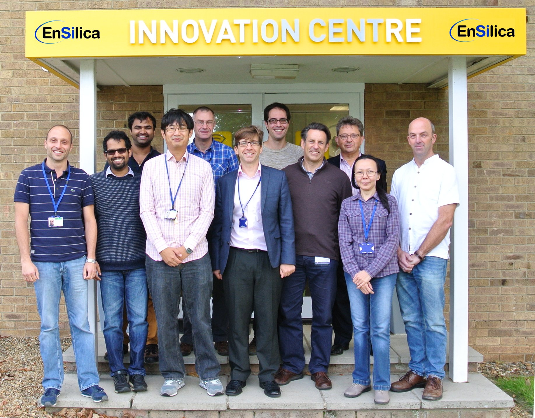
The new RF and low power sensing design centre will be headed up by Alan Wong (pictured third from left front row) who joined EnSilica from Frontier Microsystems.
Alan brought with him a design team whose pioneering experience in ultra-low power RF and sensor interfaces significantly extends EnSilica’s skills-base in addressing the needs of wireless connected IoT and wearable products.
“With their expertise covering Bluetooth low energy (BLE), near field communications (NFC) and other proprietary technologies, we are extremely pleased to welcome Alan Wong and his team to EnSilica,” says EnSilica CEO Ian Lankshear (pictured middle front row) “with the team’s proven track record of successfully delivering class-leading low power wireless SoCs and IPs for wireless personal area networks (WPAN), digital broadcast, medical bio-telemetry and other consumer applications, our new RF and sensing applications design centre has an instant head start in the market.”
The establishment of the new RF and sensing design centre grows EnSilica’s headcount to 74 staff over four design centres with around ten per cent of the staff having PhDs. It also complements EnSilica’s existing headquarters design facility in Wokingham (UK), specialist analogue and mixed-signal IC design centre in Bristol and specialist design and functional verification capabilities in Bangalore.
“The opening of our new RF and low power sensing applications design centre near Oxford is a significant step forward in the ongoing development of our semiconductor design and supply business. It perfectly complements and further extends our existing end-to-end ASIC design capabilities, including systems design, mixed-signal and digital design, embedded software, and operations, to provide us with flexible and scalable RF and sensing design expertise for IoT projects requiring custom ASIC development,” concluded Ian Lankshear.
[ad_2]
Source link