
[ad_1]
They have taken a second look at beryllium as a p-dopant for GaN.
“Experiments with beryllium doping were conducted in the late 1990s in the hope that beryllium would prove more efficient as a doping agent than the prevailing magnesium used in LED lights,” said Aalto University. “The work proved unsuccessful, however, and research on beryllium was largely discarded.”
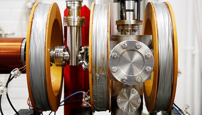
Using positron annihilation spectroscopy on a wide variety of GaN crystal types with beryllium doping, and backing this up by mathematical modelling, they have finally cracked what happens to small atom dopants in lattices made from significantly larger atoms.
While the work itself has not produce a direct route to better GaN LEDs and HEMTs, it has put another tool in the box for those working on such devices, and it looks applicable to more than just Be in GaN.
“The state-of-the-art choice for p-type doping of GaN is Mg. Remarkably, even though Mg has already been utilised as the p-type dopant in GaN devices for decades, both the exact lattice location and electronic activity of this impurity are still debated,” said the team in Physics Review Letters entry ‘Amphoteric Be in GaN: Experimental evidence for switching between substitutional and interstitial lattice sites’. “We show that Be impurities exhibit amphoteric behaviour in GaN, similar to what has been found for Li impurities in ZnO and for certain vacancy-type defects in III-V semiconductors. This finding suggests a universal property of small elements substituting for large cation atoms in these compounds, that is, the rise of a competition between substitutional and interstitial lattice sites.”
In detail, it was found that the beryllium atoms either sat between existing lattice atoms (interstitial), where they act as carrier donors, or replace atoms in the lattice (substitutional), where they act as acceptors. And that heat treatment can push the beryllium back and forth between substitutional and interstitial.
“If one wants to use beryllium, that indeed appears to have desirable properties from the point of view of manufacturing Si GaN substrates,” Professor Filip Tuomisto of Aalto told Electronics Weekly, “it is important to realise that the substrate will behave n-type during high-temperature synthesis of the substrate and p-type in high-temperature thin film deposition, changing the optimal parameter range to be used during these processes. Also, the mechanism doesn’t appear to be 100% reversible, hence multiple thermal cycling is likely to cause trouble.”
Aalto University worked with: Texas State University; the Institute of High Pressure Physics, Warsaw and the Institute of Physics PAS, Warsaw.
[ad_2]
Source link