
[ad_1]
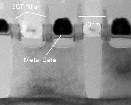
It uses surrounding gate transistors (SGTs) – a vertical gate-all-around architecture developed at Unisantis – to squeeze the cell into foot prints between 0.0184 and 0.0205μm2.
“Studies show that the vertical gate-all-around SGT-based cells have a 20-30% reduced area compared to horizontal gate-all-around FETs, while also outperforming these in terms of operating voltage, stand-by leakage and stability,” according to Imec.
Unisantis also proposes SGT-based DRAM and flash.
“SGTs have all the advantages of horizontal gate-all-around transistors, allowing a near-perfect electrostatic control of the transistor channel,” said Unisantis CTO and SGT concept inventor Professor Fujio Masuoka. “Because the channel is a vertical pillar, the concept has the potential for a significant area reduction compared to horizontal nanowire-based transistors.”
In the SRAM cell, novel design process technology co-optimisation (DTCO) achieved 0.0205μm2, using a minimum pillar pitch of 50nm. “This is a 24 percent improved scaling factor compared to the smallest SRAM designs published to date, and makes the design ready for an N5 technology node,” said Imec – a key technical challenge was ensuring sufficient pillar mechanical stability at the high aspect ratios required.
Cost could be comparable with finFET-based SRAM, if the number of process steps is kept low by using single-exposure EUV lithography, said Imec, a champion of EUV lithography.
[ad_2]
Source link