
[ad_1]

A nickel film peeled from a silicon wafer demonstrates the concept
The epitaxy grows with its crystal structure aligned with the crystalline structure of the wafer below the graphene because the weak van der Waals potential of graphene cannot completely screen the stronger potential field of substrates, said the research team in the Nature paper ‘Remote epitaxy through graphene enables two-dimensional material-based layer transfer‘.
 LEDs grown over graphene and then peeled
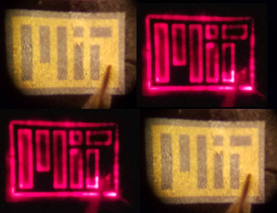
Epitaxy can be peeled off after construction because those same weal van der Waals forces leave graphene somewhat non-stick.
“We’ve had a strong belief in graphene, because it is a very robust, ultrathin, material and forms very strong covalent bonding between its atoms in the horizontal direction,” said researcher Jeehwan Kim. “Interestingly, it has very weak Van der Waals forces, meaning it doesn’t react with anything vertically, which makes graphene’s surface very slippery.”
The technique has been been proved in practice to agree with theoretical modelling on GaAs(001) on GaAs(001) substrates through, and is also applicable to InP and GaP.
Next the team plans to design a reusable ‘mother wafers’ with regions made from different exotic materials and graphene as an intermediary.
Another plan it to stack the thin structures – mixing and matching various semiconductors.
“Now, exotic materials can be popular to use,” said Kim. “You don’t have to worry about the cost of the wafer. You can grow your semiconductor device, peel it off, and reuse the wafer.”
[ad_2]
Source link