
[ad_1]
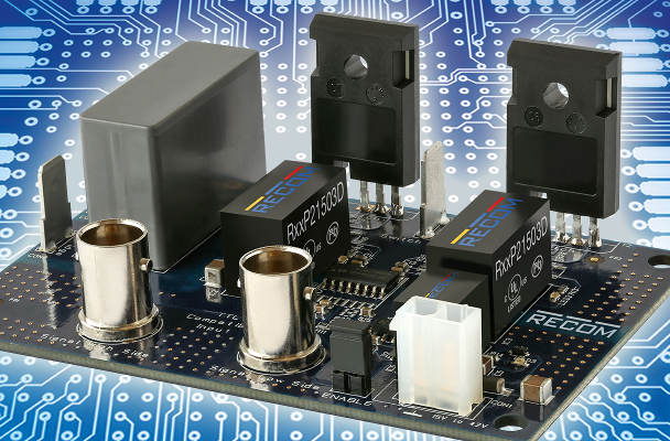
Called R-REF01-HB, the design consists of a half-bridge layout with an isolated driver stage using isolated power supplies (Recom R12Pxx) for both the low-side and the high-side switching transistors – both get both polarities so there is no problem creating bipolar drive waveforms.
Data isolation comes through a Silicon Labs Si827x, whose output is boosted through Diodes’ ZXGD3006E6TA biopolar drivers. Separate resistors allow pull up and pull down current to be adjusted independently for each output transistor.
Users can select TO247 or TO247-4L (Kelvin connected) packaged switching transistors, fit the appropriate dc-dc converter to match the transistor gate needs, then prototype and test their application.
“The reference design is a basic building block that can be used to evaluate forward, flyback, buck and boost topologies and by combining two or more units it can be used to evaluate full-bridge and 3-phase bridge circuits,” said Recom. “The PCB is optimised for high-speed switching up to 1,000V at up to 10A gate drive current.”
Signal ground is galvanically isolated from power ground, on-board BNC sockets are fitted to bring in the high speed logic control signals.
As high-side and low-side control are separate, the reference design can implement asymmetric duty cycle, active clamp and phase-shifted full-bridge topologies.
[ad_2]
Source link