
[ad_1]

Factors limiting resistance under SiC interface
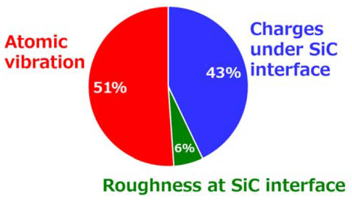
“Although it has been recognised that electron scatting under the SiC interface is limited by three factors, namely, the roughness of the SiC interface, the charges under the SiC interface and the atomic vibration, the contribution of each factor had been unclear,” said Mitsubishi.
 In a proof-of-concept, a planar SiC mosfet was fabricated in which electrons conduct away several nanometres below the SiC interface.
Not only did this show that the roughness of the SiC interface has little effect, but compared with a previous planar SiC mosfets, said the firm, resistance was reduced by two thirds owing to suppression of electron scattering because the electrons were conducting away from the charges under the SiC interface.
This is “a discovery that is expected to help reduce energy consumption in power equipment by lowering the resistance of SiC power semiconductors”, said Mitsubishi, which designed and fabricated the test device, and and analysed resistance-limiting factors. The University of Tokyo measured electron-scattering factors.
The research was revealed at the IEEE International Electron Devices Meeting (IEDM) in San Francisco this week.
Electronics Weekly has contacted Mitsubishi for more information on this research to clarify the findings.
[ad_2]
Source link