[ad_1]
This paves the way to Ge-based finFETs and gate all-around devices, as promising options for 5nm and beyond logic devices.
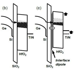
The results were achieved by band engineering using an interface dipole at high-k/SiO2 interface, and a H2 high-pressure anneal (HPA) finalizing the process flow.
The interface dipole was formed on SiO2 layer by depositing a Lanthanum (La)SiO layer by atomic layer deposition (ALD), which is a 3D-compatible process. While a high DIT has been the leading concern for Si-passivated Ge nFET, it was dramatically reduced, for the first time, from 2×1012 cm-2eV-1 down to 5×1010 cm-2eV-1 around midgap using a combination of the LaSiO insertion and a H2 HPA.
Consequently, electron mobility was increased (approximately 50 percent at peak) while PBTI reliability was improved thanks to the interface dipole-induced band engineering.
Imec has modelled heterostructure interface resistivity (Rhi) analysis for highly doped semiconductors. Using this model, Imec predicted that high-doping Si:P in a TiSix/Si:P/n-Ge contact stack helps to overcome the high contact resistance problem in Ge nMOS.
With development of an advanced low-temperature Si:P epitaxy technique, imec demonstrated a TiSix/Si:P/n-Ge contact stack with record-low contact resistivity for n-Ge.
“Dedicated to push the boundaries of Moore’s law, Ge-based devices are a key focus area or our research,” says Imec’s An Steegen, ‘these breakthrough achievements underscore our dedication to understanding the fundamental roadblocks that need to be overcome in order for Ge-based devices to become a viable solution for 5nm and beyond.”
[ad_2]
Source link

