
[ad_1]
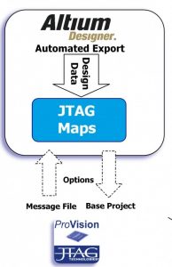 Called JTAG Maps it is available as a free extension for the Altium Designer tool.
Boundary-scan device models (BSDLs) are used for JTAG/boundary-scan testing as they indicate which pins can be controlled or observed.
BSDL models may not always be available so the companies have included in JTAG Maps an ‘assume scan covered’ feature enabling a view of potential boundary-scan coverage without a specific BSDL.
This feature can also be used to indicate fault coverage to a connector (set to assume scan covered) or to highlight the differences in fault coverage between two equivalent parts, one with and one without built-in JTAG/boundary-scan.
JTAG Maps for Altium will automatically detect the scan chain path (or paths) with no limits to the number of paths (aka TAPs) in the design. The nets associated with the TAPs will be highlighted separately from the ‘testable’ nets.
Another features of the tool is that after exporting a JTAG ProVision project, the data can be sent to your local JTAG Technologies office, Approved Application Provider, or approved JTAG representative for further analysis.
[ad_2]
Source link