
[ad_1]
Bold claims. Can the company justify them?
Yes, according to Plessey product line manager Clive Beech and applications engineering manager Leon Baruah, who took time out to tell Electronics Weekly how.
At its fab in Plymouth Devon, Plessey has been developing LEDs whose all-important photon-emitting GaN layers are grown on conventional silicon substrates rather than expensive sapphire or silicon carbide.
Because the lattice spacing is far from ideal, this is not easy.
What makes it possible, are a series of buffer layers that not only gradually change the lattice constant from silicon to GaN spacing, but also balance stresses that would otherwise curl the wafer up like a Pringle.
It acquired its basic buffer-layer intellectual property with the purchase of Cambridge University spin-out CamGaN in 2012 and has subsequently converted the concept into a manufacturing process that can produces efficient powerful LEDs.
Always a theoretical possibility, the cheaper substrate and chip experience really has led to cost reduction, says Plessey, leading to the 50% cheaper claim above.
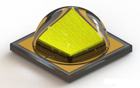
Four junction 12V 700mA PLW7070GA without phosphor, lit with a tiny current
“Especially in these high-power applications, the die is a significant proportion of cost, and our die is cheaper,” says engineering manager Baruah. “Our process is also quite automated because we use standard silicon semiconductor manufacturing technology, while theirs [competitors’ processes] are quite manual. In volume, if you are considering that a typical 7070 can be sold for $2.50-3.00, we sell our packaged part for $1.50.”
 Standard IC manufacturing equipment and expertise is available for automation at the Plymouth LED fab because the same facility spent many years making ICs.
Not only has chip-making heritage helped with this, but it also helped to get over another bug-bear of high-power LEDs – cross-hairs (diagram below).
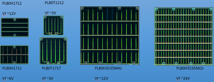
Generally, a 12V LED has four wire-bonded die arranged in a square on a substrate. Because of the way these are packaged, there are inevitably gaps between the die, resulting in a non-emissive cross-shape in the middle of the emissive area.
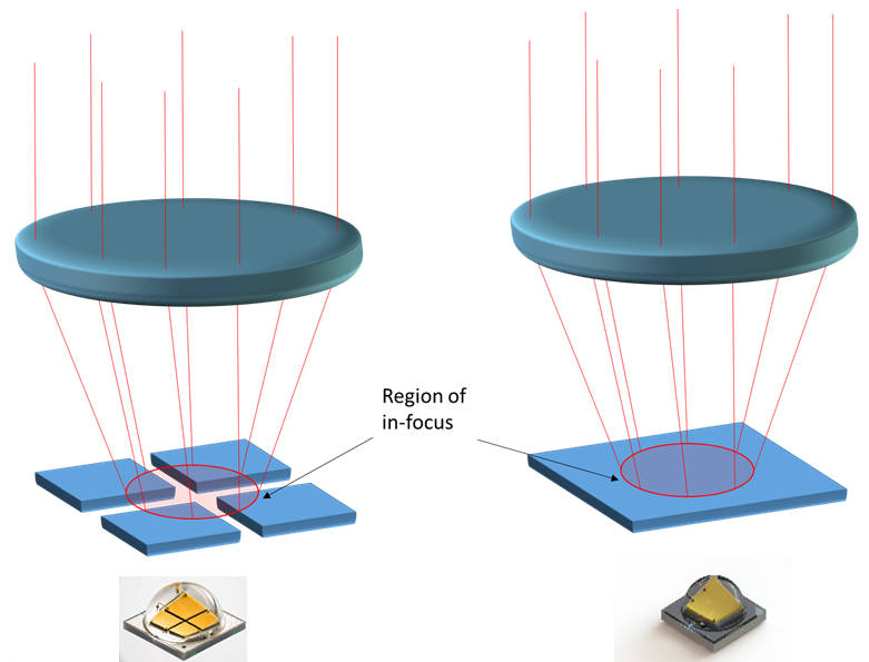 Once secondary optics are added, particularly narrow beam optics, the dark centre of the cross is imaged into the beam creating a hole-in-the-middle effect.
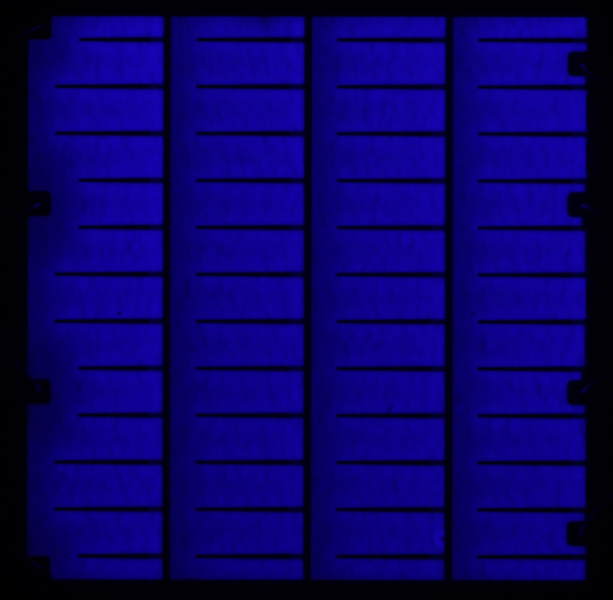
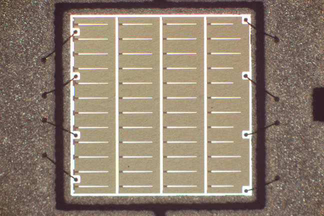
By tiling four LED junctions monolithically using its chip-making experience, Plessey has reduced these gaps to microscopic proportions – hair-lines so thin that they make no visible difference to emission – so no hole in the middle, nor imaged cross-hairs.
As it happens, the PLW7070 has four 0.5 x 2mm junctions side-by-side (see diagram below), but the narrow gap argument still applies. To connect them in series, current is bought from the top of one junction to the bottom of the next using integrated circuit techniques (see diagram above), and wire-bonding is only needed at the edge of the quad-junction die.
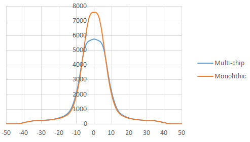 It is the lack of gaps that that leads to the 30% increase in light output claim comes from – the Plessey LED develops 30% more centre-beam candlepower compared with four separate die in a package (see graph right), according to product manager Beech. “One customer has a 2° [+/-1°] light fixture and can’t use four-die, so he uses an expensive large-die 3V chip running at 3A. With our 12V 700mA LED, he can buy 10 of ours for one of theirs, and he gets easier routing because the current is lower.”
The monolithic junction tiling concept, which uses SiO2 layers to isolate the die from the substrate (see cross section), can be extended a long way.
 “For 24V, we can put eight stripes on a single silicon die with no need to mechanically interconnect,” says Beech. “The oxide thickness is important – it needs to be thicker for more isolation. In theory, we could make a 240V LED by tiling 80 junctions.”
To make the LEDs, Plessey grows the GaN junction up-side-down, then wafer-transfers to a second wafer to bring the emissive surface to the top (see cross section[again: slide 4 left]). Having access to both sides of the GaN allows electrical interconnection to be achieved.
“The whole process relatively complicated, but we can go from bare silicon wafer to LEDs giving out light in 7-10 days, compared with the six weeks it took when we used to make CMOS,” says Beech. “CMOS has around 30 mask steps in manufacture, and for LEDs we have seven with not-particularly-critical alignment. It is a very tolerant process.”
The 7070 package is also novel. While sitting on an industry-standard footprint, aluminium nitride ceramic construction has allowed thermal resistance to be pushed below 2°C/W.
Because GaN-on-Si is unusual, and package is new, the company has put considerable effort into reliability testing – more than is usual in the LED industry, claims Beech.
“Silicon is very robust and mechanically very strong,” he says. “We used to make high-reliability CMOS in the fab, and so we have gone through a whole set of reliability tests like we would have done in CMOS, and it [the LED] got a clean bill of health.”
“Temperature cycling is particularly robust,” he continued, “It sailed through – partly because it is a silicon device. It is at least as good as sapphire and silicon carbide.”
An earlier 3535 (3.5 x 3.5mm) LED based on the same technology has had a particular hammering in trials,
“We have been especially aggressive as we want to be sure we are not going to have reliability issues,” says Beech. “We are running the 3535 at four times the current density of 7070 – it was designed for 20A/cm2 and it was running at 60A/cm[super2] during environmental testing.”
The 7070 is going through standard LM80 (lumen maintenance: time to 80% of initial output) testing, driven at nominal current, at 55, 85, 105°C, according to engineering manager Baruah. “We have also done the tests at absolute-maximum current, which is not the case at most manufacturers,” he says. “We need at least 6,000 test hours as then we can extrapolate six times to 36,000 hours.”
So far, the 7070 LEDs have clocked up over 4,000 hours at 700mA (~8.5W) and lumens are at 96% initial value, according to Beech. 5,000hr will be crossed in two weeks, with 6,000hr in April.
In parallel, over-drive test at 15W are in progress. All at an independent test house.
“The device is behaving systematically smoothly, with no unusual behaviour,” says Beech. “The maximum level curves are almost indistinguishable from typical, which shows it doesn’t really care – degradation is not a strong function of power.”
When the firm started producing GaN-on-Si devices two or three years ago, it put some into 3020 PLCC packages (part PLW114050) and began long-term 85°C tests at 60mA, equating to 35A/cm2.
So far, 40 of them have clocked-up 14,000 hours.
“Most of industry runs at 15A/cm2,” says Beech, “and it’s a much harsher test because it’s a plastic package so die temperature is higher.” PLCC thermal resistance is ~30K/W.
Output deteriorated steadily to just above 70% of initial output at 11,000 hours, where it levelled out. The take-away message is, says Beech, that “this is not a technology that is going to fall off a cliff.”
Over the same time, blue (non-phosphor) versions settled to ~80% after 3,000h and have been there ever since.
These early 3020 white LEDs had standard phosphors, poured into the package, but over the last 18 months Plessey has built up its own phosphor capability – based on buying-in individual phosphors and blending on-site.
“We have specialists who can engineer our phosphors,” says Beech, “Our engineers mix them here and we have our own assembly line – its limited manufacturing here, and volume in the Far-East.”
Mostly phosphor application today, he added, is thin-film spraying of either a mixed phosphor, or multiple layers of separate phosphors.
Close behind the 12V four-junction 7070 in the product pipeline is a 3V version on the same size chip. “The core engineering work is done. Reliability likely to be the same as the 12V,” says Beech. A 24V version is also mooted.
As an aside, he claims GaN-on-Si has another advantage over sapphire. “With sapphire, the light passes through the volume of the substrate where it bounces around and gets losses. GaN-on-Si can make bigger and bigger die because the LED is on the top surface, so it doesn’t suffer from sapphire losses.”
However good and cost-effective cheap these high-power large-area GaN-on-Si LEDs are, they are unlikely able to compete on price against chip-on-board emitters in wide beam applications.
“This product is never going to be designed into a down-lighter or a troffer,” says engineering manager Baruah.
Where they can win is where optical physics rules out CoB solutions – where a narrow or intricate beam has to be delivered from a small package.
The minimum diameter of secondary optics is proportional to emitter diameter – so fat CoBs need bulky optics, where a 7070 with a 2x2mm die can have compact optics.
“We are looking at directional lights with narrower beams, like spotlights; streetlighting which needs very particular light distribution; and projector lights,” says Beech.
Plessey PLW7070GA at a glance
- 7070 aluminium nitride pacakge
- <2K/W
- 350mA to 3A (1-15W)
- 135°Cmax junction
- 12V (24V and 3V in pipeline)
[ad_2]
Source link