
[ad_1]
Features include:
- Encryption key protection
- Hardware encryption accelerators for AES, 3DES, and SHA
- true random number generator
- Protect boot code storage
“The expanded RX65N/RX651 devices support security and reprogrammability needs, offering integrated enhanced flash protection, and other technology to create a secure and stable integrated solution, as proven by the Cryptographic Algorithm Validation [CAVP] certification,” said the firm.
For human-machine interface, the two ranges include a TFT controller and 2D graphic acceleration.
“Selecting a WQVGA display allows the 640kbyte of on-chip RAM to be used as display frame buffer, which saves external RAM,” said Renesas.
The RXv2 core and 40nm process allow 4.55 Core Mark/MHz performance.
Using the new security features, according to the firm, end users will be able to:
- Monitor the operating state of machinery from inside and outside a factory
- Exchange data for making changes to production instructions
- Reprogram the MCU’s memory to update equipment settings
Dual bank flash is included to support in-the-field firmware updates.
There is a board support package, which controls the common information for functions like initial MCU, clock, and board settings, and “the new Envision Kit provides an evaluation environment that allows engineers to benchmark MCU performance and start developing their own software,” said Renesas.
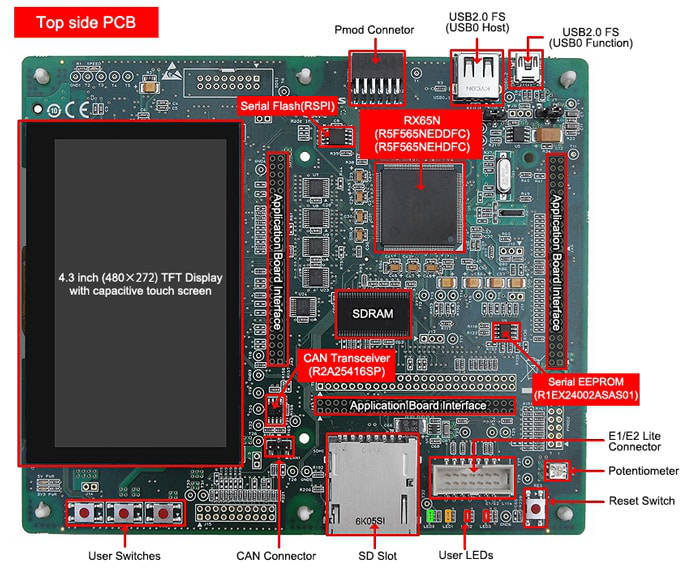
The RX65N starter kit includes a development board with MCU, display, on-chip debugger, trial C compiler and integrated development environment.
| Code flash
1.0Mbyte or less |
Code flash
1.5Mbyte or more |
|||||
|---|---|---|---|---|---|---|
| RX65N | RX651 | RX65N | RX651 | |||
| CPU | RXv2 | |||||
| Frequency | 120MHz | |||||
| Vcc | 2.7 – 3.6V | |||||
| Memory | Code Flash | 512, 768kbyte, 1Mbyte | 1.51,2.01Mbyte | |||
| Dualbank function | – | Yes | ||||
| BGO function | – | Yes | ||||
| Data Flash | – | 32kbyte | ||||
| SRAM | 256kbyte | 640kbyte(256+384) | ||||
| DMA | DMAC x 8 channels, Data Transfer Controller (DTC), EXDMAC x 2 channels | |||||
| External Bus | 8/16bit separate/multiplex, SDRAM | 8/16/32bit separate/multiplex, SDRAM | ||||
| Timer | General Purpose Timer | Multi-function timer unit (MTU3):
16bit x 8 channels +3 2bit x 1 channel 16bit x 6 channels 8bit x 4 channels 16bit(CMT) x 4 channels + 32bit(CMTW) x 2 channels |
||||
| RTC with battery back-up | 1 channel | |||||
| Indepedent watchdog / watchdog | 1 channel / 1 channel | |||||
| Communication Interface | Serial comms interface /
Serial comms interface with FIFO |
11 channels / 2 channels | ||||
| I²C bus | 2 channels | 3 channels | ||||
| SPI | 3 channels | |||||
| Quad serial peripheral interface | 1 channel | |||||
| Ethernet, EDMAC | 1 channel | – | 1 channel | – | ||
| USB2.0 full speed | 1 channel (host/function/OTG) | |||||
| CAN | 2 channels | |||||
| SD host interface/
SD slave interface |
1 channel / 1 channel | |||||
| MMC host interface | 1 channel | |||||
| Analog | ADCs | 12bit x 8 channels (with 3ch S&H) + 12bit x 21 channels |
||||
| DACs | 2bit x 2 channels | |||||
| Security | AES | Yes | Yes (Built in Trusted secure IP) | |||
| True random number generator (TRNG) | Yes | Yes (Built in Trusted secure IP) | ||||
| Trusted Secure IP | – | Yes | ||||
| Human machine interface | CMOS camera interface | PDC (parallel data capture) |
1 channel | |||
| Graphic | Graphic LCD controller | – | 1 channel | |||
| 2D drawing engine | – | Yes | ||||
| Other | CRC32, Data operation circuit, port output enable 3, event link controller, temperature sensor | |||||
| Package | 100 LFQFP (0.5mm pitch, 14x14mm) 144 LFQFP (0.5mm pitch, 20x20mm) 100 TFLGA (0.65mm pitch, 7x7mm) 145 TFLGA (0.5mm pitch, 7x7mm) |
|||||
| – | 176 LFQFP
(0.5mm pitch, 24x24mm) (0.8mm pitch, 13x13mm) (0.5mm pitch, 8x8mm) |
|||||
[ad_2]
Source link