
[ad_1]
Some of it I have failed to work out yet, and all the bits I have worked out, I am impressed with.
It is an all-silicon design, apart from the CRT, with BC107s doing much of the work – for no good reason, I would have thought RF transistors would be used in a 10MHz scope.
That said, wise analogue guru Jim Williams (coincidentally lover of Tek scopes) said never use a transistor that faster than you need, because faster transistors open the door to problems like oscillation.
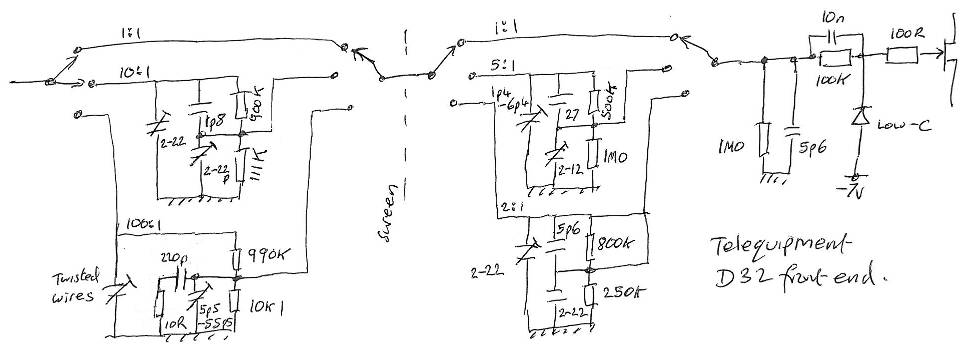
Anyway, one of the bits I sort of understand is the front end – see my sketch of the digram (redrawn because Tek drew it out in a spidery way).
BTW, there is a switchable 100n in series before the left hand side to allow ad or dc coupling. The fet on the right is a source follower, and the low-capacitance diode, 10n and 100k are input overload protection. The source follower feeds a differential pair with offset (x-shift) control feeding the other side.
Please forgive me if I have mis-transcribed any of the values
The second-stage 2:1 and 5:1 are used in conjunction with either 1:1, 10:1 or 100:1 at the front to get all the attenuation values.
The two 100:1 potentiometer resistors are a single device, and the 10:1 resistors are another single device. Then the 1M, both the 5:1 resistors and the 2:1 resistors are all in one device – matched to sort out dc accuracy.
What slightly boggles my mind is the thought of adjusting all those capacitors to get an accurate response over frequency and over all the combinations of potentiometers needed across the vertical ranges.
I can’t work out which one to adjust first, and am surprised that there are any fixed capacitors at all – any external wisdom would be appreciated.
My guess is that in modern scopes the designers have got to grips with capacitance and use only fixed values, and that these are some how adjusted for the semiconductor switches that are now used instead of mechanical switches (that said, the ac/dc switch in many modern scopes still seems to be a relay.
UPDATE: Having found several schematics (here), here, here, all linked from this forum – thanks) on the web, they all use small relays (prob latching for low power) to switch the front-end attenuators.
Further update: on the same forum, read the two articles scanned by ‘Liv’ – gold dust.
That said, the low-end (but seemingly decent) DS212 pocket scope in the video linked to in the earlier scope blog uses a couple of HC4053 (CMOS 3pole 2way) analogue switched plus an RC network including two trimmer caps per channel.
 Texas Instruments has a design note that mostly covers a high-performance 50Ω scope input stage, but also had a high-z input buffer (figure 68) and a 100:1 10:1 input attenuator to go with it (figure 69). The buffer is again a source follower, and fractional gains come through switching the attenuation (1:1 <> 10:1 in 10 2dB steps) of the following LMH6518. This chip is designed for scope front ends and includes a separate amplifier for the trigger signal chain.
The text associated with figure 69 says the RC time constant of the top of a potentiometer should match the lower RC, and then the parallel capacitor should be adjusted so the scope input capacitance is the same on each range, so maybe this is my answer, and this is why only one capacitor is adjustable on each of the Tek/Tele D32 potentiometers.
[ad_2]
Source link