[ad_1]
The Leti-coordinated COSMICC project will combine CMOS electronics and Si-photonics with high-throughput, fiber-attachment techniques.
These scalable solutions will provide performance improvement an order of magnitude better than current VCSELs transceivers, and the COSMICC-developed technology will address future data-transmission needs with a target cost per bit that traditional wavelength-division multiplexing (WDM) transceivers cannot meet.
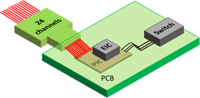
For example, the project’s 11 partners from five countries are focusing on developing mid-board optical transceivers with data rates up to 2.4 Tb/s with 200 Gb/s per fiber using 12 fibers. The devices will consume less than 2 pJ/bit. and cost approximately 0.2 Euros/Gb/s.
“By enhancing an R&D photonic integration platform from project member STMicroelectronics, the partners in COSMICC aim to demonstrate the transceivers by 2019,” says Leti’s Ségolène Olivier, “we also plan to establish a new value chain that will facilitate rapid adoption of the technologies developed by our members.”
Several technological developments will be used to boost the photonic integration platform’s high data-rate performance, while also reducing power consumption.
A first improvement will be the introduction of a SiN layer that will allow development of temperature-insensitive MUX/DEMUX devices for coarse WDM operation. In addition, the SiN layer will serve as an intermediate wave-guiding layer for optical input/output to and from the photonic chip.
Additional steps will enhance modulator performance to 50 Gb/s, while making the transceivers more compact and reducing energy consumption.
The partners will also evaluate capacitive modulators, slow-wave depletion modulators with 1D periodicity, and more advanced approaches. These include GeSi electro-absorption modulators with tunable Si composition and photonic crystal electro-refraction modulators to make micrometer-scale devices.
In addition, a hybrid III-V on Si laser will be integrated in the SOI/SiN platform in the more advanced transmitter circuits.
Project demonstrators will be tested in both lab and field environments.
Project participants include ST, University Pavia (Italy), Finisar (Germany), Vario-Optics (Switzerland), Seagate (UK), University Paris-Sud (France), University St. Andrews (UK), University Southampton (UK) and Ayming (France).
[ad_2]
Source link

