[ad_1]
by Gary Dagastine
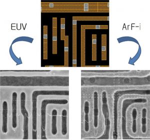
 Samsung EUV lithography demonstrated better fidelity to the mask pattern than traditional argon fluoride (ArF) lithography
The company used EUV, along with additional front-end scaling, special design constructs and a single diffusion break, to build transistors with a fin pitch and contacted polysilicon pitch (CPP) of 27nm and 54nm, respectively, demonstrating a 50-60% reduction in power requirements versus the company’s 10nm technology. Samsung built a 256Mbit SRAM array with a cell size of just 0.0262µm2 from these devices, along with CPU/GPU logic circuits, all of which met NBTI reliability requirements.
Separately, the company detailed a low-power 8nm FinFET logic technology for mobile, high-performance and low-power applications. An extension of its existing 10LPP (“Low Power Plus”) 10nm process in volume production, the new 8LPP process consumes 7% less power, is some 15% smaller in area, and can operate at 0.35V. These improvements are due to continued scaling of gate lengths and fin profiles, along with reduced contact resistance and a better sub-threshold leakage profile.
As if two new advanced manufacturing processes weren’t enough, Samsung took the wraps off yet another, which it claims offers the most competitive device performance and aggressive gate pitch (78nm) in the foundry business at technology nodes larger than 10nm. The low-power, high-performance 11LPP platform technology is for mobile and GPU applications. It adopts and enhances features from the company’s existing 14nm and 10nm technologies and incorporates updated design rules. In a ring oscillator test circuit, device performance was shown to be 25% better than Samsung’s 1st generation 14nm finFET technology. (Or if performance was held the same, then power consumption was 42% less.)
Globalfoundries weighs-in
Meanwhile, Globalfoundries unveiled a 12nm FinFET technology for low-power, high-performance applications. An evolution of its 14nm 14LPP technology, the new 12LPP process reduces area and power requirements by 10% and 16%, respectively, or it can deliver a 15% performance improvement at a given leakage, all with comparable reliability and yield. In addition, SRAMs built with the new process benefit from a 30% leakage reduction.
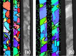
Separately, Globalfoundries posed and answered the question, how can the use of copper interconnect be extended as scaling proceeds? The problem is that resistance in copper lines increases as line-widths shrink because of electron scattering at grain boundaries, surfaces and interfaces. Company researchers described a nanosecond flash anneal process that increases copper grain sizes, thereby removing many of these boundaries and interfaces, and providing a better interface between the copper and barrier layers, thus a less resistive path for electrons.
 Copper interconnect before (a) and after (b) Globalfoundries’ nanosecond laser anneal.
Left in each image is copper grain orientation
Middle is copper grain phase
Right is transmission electron microscope photo
All show that copper lines have larger grains and fewer troublesome grain boundaries and better interfaces after the anneal.
The result is a 35% reduction in resistance, giving a 15% improvement in RC delays and a gain in on-current (IDsat) of 2–5%. In addition, breakdown voltage and copper reliability were enhanced. However, the company said the process, while useful for the most critical metal levels, may not be economical for all levels.
A step toward practical quantum electronics
CEA-Leti led the conference into an entirely different realm: the world of quantum electronics. Manipulating the “spin” of electrons and holes in silicon holds promise as the basis for quantum computing, which one day may be used to solve problems beyond the reach of today’s supercomputers. However, in order to make quantum computing practical and to be able to scale it up in manufacturing, a way must be found to control electron/hole spin electrically, and not with complex hybrid co-integrated micromagnet/electrical schemes.
As a step toward doing this, CEA-Leti disclosed it has experimentally demonstrated the first electric field-mediated control of the spin of holes in silicon, using a SOI quantum dot device fabricated in a standard CMOS process flow. The underlying control mechanism is based on a complex interplay between spin-orbit coupling and the conduction band of silicon, enhanced by the device’s geometry.
MRAMs, and More MRAMs
As the industry moves to smaller nodes, the scaling of SRAM memory for embedded last-level-cache (LLC) applications becomes challenging and the search is on for alternatives. Spin-transfer-torque magnetic random access memory (STT-MRAM) has shown great promise given its speed, endurance and suitability for back-end integration, but its relatively high operating voltage is a concern.
However, TDK-Headway researchers detailed at VLSI 2018 the first STT-MRAM capable of low-voltage, low-power operation. By cleverly engineering the tunnel barrier in 30nm devices, they achieved writing voltages as low as 0.17V (for a 1ppm error rate), 20ns writing operation and 35µA writing current. They say further improvements are possible.
Samsung described an embedded STT-MRAM built in a 28 FD-SOI process. It operates across the full industrial temperature range (-40ºC to 125ºC) and exhibits high endurance and more than 10 years of data retention. Memory cell operation is said to be robust in solder reflow conditions and under external magnetic disturbance.
Globalfoundries, with an eye toward automotive applications, unveiled a fully functional embedded MRAM (eMRAM) integrated into a 22-nm FD-SOI CMOS process flow. It demonstrated a bit error rate of less than <1 ppm after five solder reflows, met the automotive grade-1 data retention requirement, and demonstrated high intrinsic stand-by magnetic immunity. The researchers say these results indicate eMRAM is capable of serving a broad spectrum of eflash applications at 22 nm or beyond.
TSMC unveiled a 16Mb embedded MRAM reference and sensing circuit in a 40nm CMOS logic process that addresses a key problem with MRAM devices: a small read window, arising from MRAM’s small tunnel-magneto-resistance ratio. TSMC addressed this problem with a hybrid-resistance-reference and novel cell configuration. The measured results show better than 1µA sense resolution and a speedy 17.5ns access time from -40ºC to 125°C.
Autonomous mini-drones
Finally, autonomous, miniature drones are on their way. A Massachusetts Institute of Technology team described a chip they call Navion, which enables autonomous navigation of miniaturized robots such as nano drones.
Said to be the first fully integrated visual-inertial odometry (VIO) chip, Navion is an asic fabricated in 65nm CMOS and co-designed in tandem with the algorithms which run on it. It uses inertial measurements and mono-stereo images to estimate a drone’s trajectory, as well as to generate a 3D map of its environment. On-chip integration of these functions reduces energy and footprint, and eliminates costly off-chip processing and storage. It can process 752×480 stereo images at up to 171fps and inertial measurements at up to 52kHz, and is configurable to maximize accuracy, throughput, and energy-efficiency across various environmental conditions.
Gary Dagastine attended the recent Symposia on VLSI Technology and Circuits in Honolulu.
This year more than 900 scientists, engineers and technologists attended the annual event, which alternates between Hawaii and Kyoto, Japan. It was the highest attendance in 12 years, a noteworthy inflection given the increased cost and difficulty of continued scaling according to Moore’s Law.
And, following the path of Moore’s Law is just one approach. “We have broadened our views on how to move forward,” said Maud Vinet, VLSI committee member and manager of the Advanced CMOS Laboratories at Grenoble-based CEA-Leti. “There are lots of tricks available in terms of materials and new architectures that will help us continue to serve up innovations.”
[ad_2]
Source link
