[ad_1]
Wafer-to-wafer bonding is a promising technique for enabling high-density integration of future ICs through 3D integration.
This is achieved by aligning top and bottom wafers that are then bonded, thus creating a stacked IC.
An important advantage is that wafers/ICs with different technologies can be stacked, e.g. memory and processor ICs.
Many of the alignment techniques and bonding methods for 3D integration have evolved from microelectromechanical system (MEMS) fabrication methods.
The fundamental difference between MEMS and 3D integration is that the alignment or overlay accuracy has to be improved by 5–10 times.
Accurate overlay is needed to align the bonding pads of the stacked wafers and it is essential to achieving a high yield with wafer-to-wafer bonding. Imec and EVG have realized excellent results on overlay accuracy.
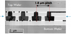
Firstly, the hybrid (via-middle) wafer-to-wafer bonding technique was improved by using EVG’s high quality bonding system with beyond state-of-the-art integration definition of bonding pads, resulting in a high yield and a 1.8µm pitch, which is significantly better compared to recently published results at recognized conferences such as ECTC and 3DIC reporting 3.6µm pad size.
Secondly, the dielectric (via-last) wafer-to-wafer bonding technique was tackled. This technique requires extremely good overlay accuracy to align the copper pads from both wafers, which are then contacted by through-silicon vias (TSVs). In this case, 300nm overlay across the wafer was achieved.
“Further improving the overlay accuracy for wafer-to-wafer bonding into the sub-200nm range requires optimization of the interaction between the wafer bonding tool and processes as well as pre-and post-processing and the wafer material,” says EVG’s Markus Wimplinger.
Imec’s 3D integration program explores technology options to define innovative solutions for cost-effective realization of 3D interconnect with TSVs.
Imec’s 3D integration processes are completely executed on 300mm.
Imec also explores 3D design to propose methodologies for critical design issues, enabling effective use of 3D interconnection on system level.
[ad_2]
Source link

