
[ad_1]
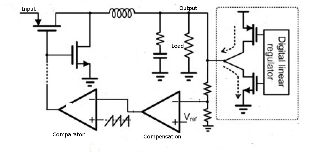
Figure 1: Linear assistance can improve DC-DC transient response, but the question is when to apply it
Simple linear assistance can cut transient errors in DC-DC converters without wrecking stability, according to the Hong Kong University of Science and Technology.
It described a 30MHz DC-DC converter at the IEEE International Solid State Circuit Conference (ISSCC) in San Francisco. Its output deviates only 36mV, and settles to 1% within 125ns, following a 1.25A 2ns load transient.
The challenge with linear assistance is deciding how to control when that assistance is applied.
A simple voltage comparator on the output is one scheme, but setting its threshold becomes a difficult compromise between effective support and ignoring noise.
In the Hong Kong scheme, which is based on a voltage-mode PWM loop, the DC-DC converter is already agile without assistance because unity gain bandwidth is set to around 30MHz/5 using a Type-III compensator.
“When there is an abrupt large load change, the compensator responds promptly, and the output of the compensator [Vc in Figure 1, above] may even jump higher than the range of the ramp signal and saturate the duty cycle to D=1,” said the university. “By having D=1 and the optimised unity gain bandwidth, the PWM control scheme achieves near-optimal transient responses.”
It is this flighty response that is exploited to control assistance.
With the upper buck transistor fully on (at D=1), rate of current rise is limited by the inductance, and extra current would be welcome.
So the transition into PWM saturation is detected by comparing the PWM input voltage with the upper and lower limits of the PWM reference sawtooth.
This extra comparison circuitry (not shown in the diagram) is used to switch on the linear current supply (right‑hand mosfets), with the magnitude of assistance set by measuring Vc.
“As Vc is an internal node, it has a much better noise immunity than the output voltage, and monitoring Vc can reduce under-shoot and over-shoot more effectively,” said the university.
The Hong Kong paper (ISSCC 2017 10.6) goes on to describe the compensation scheme, developed to smoothly add linear assistance for fast response, while maintaining stability.
“The converter is free from both small-signal and sub-harmonic oscillations,” said the university, which has proved the scheme in a 0.13µm CMOS chip.
Also at ISSCC, IBM and MIT have aimed at low-power applications with a DC-DC converter that requires only 240pW quiescent power, peaks at 92% efficiency and has a >1,000,000:1 dynamic range.
It can convert 1.2V-3.3V (2V nominal) at its input to 0.7V-0.9V (0.8V nominal) for loads spanning 100pA to 1mA.
“Power conversion in increasingly constrained systems requires extremely low quiescent power in sleep mode to enhance lifetimes,” said the team, in ISSCC paper 10.8.
“At the same time, a wide dynamic range without compromising efficiency is required to handle heavily duty-cycled loads or varying power from energy-harvesting sources,” it said.
Its design is constrained by a series of consequences.
Drain is so low that the leakage of ceramic capacitors becomes significant, so to keep their leakage below 50pW, Cout and Cin had to be limited to 350nF and 150nF respectively.
With an output ripple limit of 10mV, this low capacitance constrains energy per switching cycle to around 1nJ-2nJ. And with a 47µH inductor, peak current therefore needs to be under 10mA.
10mA means the power fets were allowed on-resistance around 3Ω-5Ω, and it was possible to design them to achieve this, hit the speed specification, and only leak about 40pW.
Speed is set by output power demands where the above 1nJ-2nJ needs to be delivered at frequencies from 1Hz to 1.2MHz.
Then, according to the paper, the design challenge became to maintain efficiency by developing control circuits that draw power proportional to clock frequency, while minimising leakage.
Creating a PWM to operate over such a huge dynamic range, while taking proportional power‑draw into account, meant switching multiple oscillators – optimised for different frequency ranges – through a programmable divider, plus generating the variable pulse width already mentioned.
Oscillators are RC types with fixed R and banks of switchable capacitors. For example, the pulse-width generating monostable has 160kΩ and a 0pF‑3.2pF binary-weighted capacitor bank to provide 400ns tuning range in 6ns steps.
Among many other power‑saving schemes, the feedback resistor pair is disconnected from the output by a fet between samples.
Efficiency is held at >80% for loads between 10nA and 1mA for all input voltages – and at >90% for the same load range at Vin=1.2V.
[ad_2]
Source link