
[ad_1]
Imec also presented novel designs that would allow using mono-layer 2D materials to enable Moore’s law even below 5nm gate length.
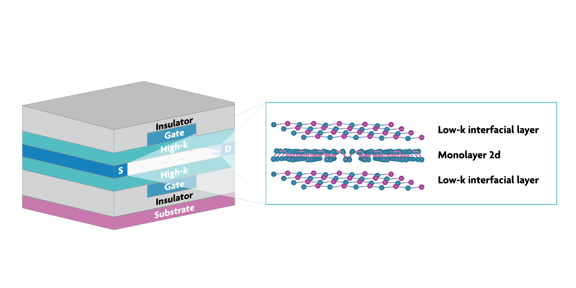
2D materials, a family of materials that form two-dimensional crystals, may be used to create the ultimate transistor with a channel thickness down to the level of single atoms and gate length of few nanometers.
A key driver that allowed the industry to follow Moore’s Law and continue producing ever more powerful chips was the continued scaling of the gate length. To counter the resulting negative short-channel effects, chip manufacturers have already moved from planar transistors to FinFETs.
They are now introducing other transistor architectures such as nanowire FETs. The work reported by imec looks further, replacing the transistor channel material, with 2D materials as some of the prime candidates.
In order to fit FETs based on 2D materials into the scaling roadmap, it is essential to understand how their characteristics relate to their behavior in digital circuits.
Imec scientists havevpresented guidelines on how to choose materials, design the devices and optimize performance to arrive at circuits that meet the requirements for sub-10nm high-performance logic chips.
Their findings demonstrate the need to use 2D materials with anisotropicity and a smaller effective mass in the transport direction. Using one such material, monolayer black-phosphorus, the researchers presented novel device designs that pave the way to even further extend Moore’s law into the sub-5nm gate length.
These designs reveal that for sub-5nm gate lengths, 2D electrostatics arising from gate stack design become more of a challenge than direct source-to-drain tunneling. These results are very encouraging, because in the case of 3D semiconductors, such as Si, scaling gate length so aggressively is practically impossible.
“2D materials, with the atomically-precise dimension control they enable, promise to become key materials for future innovations. With advancing R&D, we see opportunities emerging in domains such as photonics, optoelectronics, (bio)sensing, energy storage, photovoltaics, and also transistor scaling. Many of these concepts have already been demonstrated in the labs,” says Imec’s Iuliana Radu, “our latest results show how 2D materials could be used to scale FETs for very advanced technology nodes.”
[ad_2]
Source link